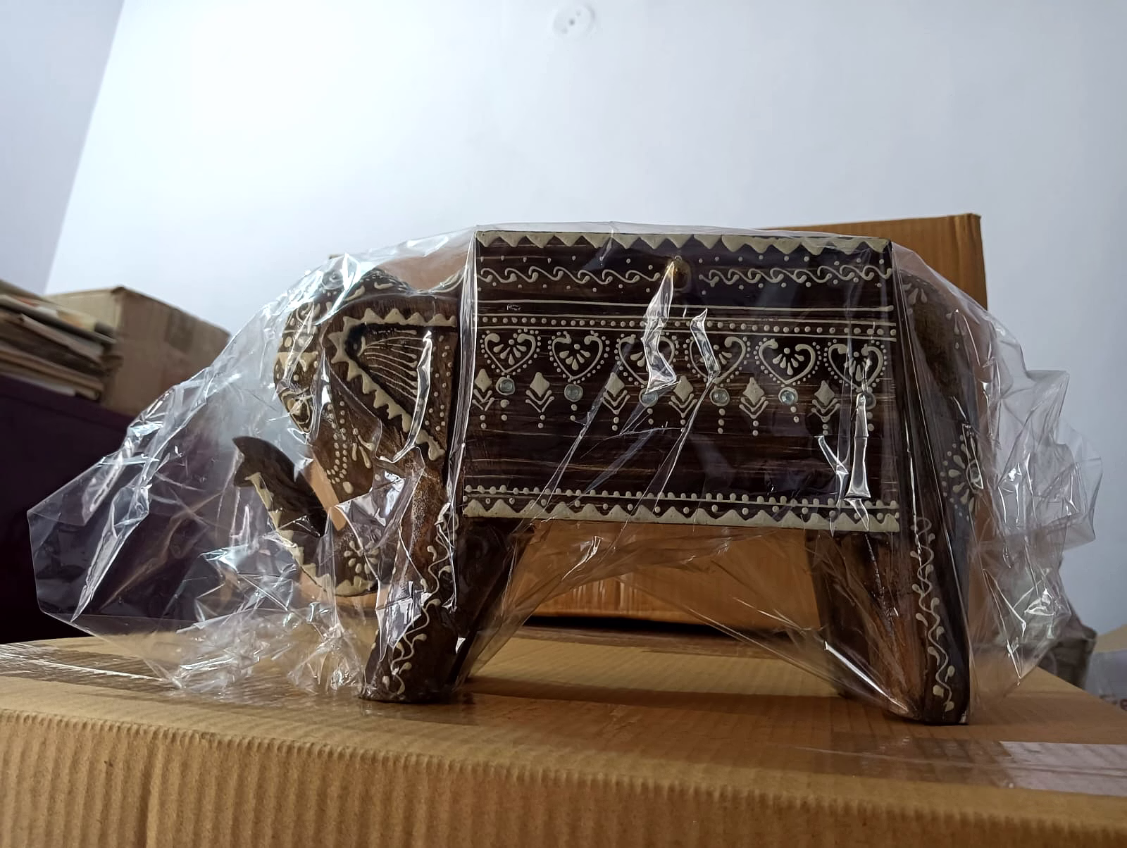
The 2 Inch Single Side Polished Silicon Wafer is a premium semiconductor-grade product specifically designed for high-precision research, development, and sophisticated electronic device fabrication. Manufactured with N-Type silicon and a precise <100> crystal orientation, this wafer exhibits exceptional electrical properties and a uniform crystal structure, which are critical for microfabrication processes, nanotechnology development, and advanced semiconductor applications. The wafer features a thickness of 280 microns and a resistivity range of 1-10 ohm-cm, optimized for performance in etching, chemical vapor deposition (CVD), physical vapor deposition (PVD), and lithography processes. Its single-side polished surface ensures ideal flatness and minimal defects on the working side, essential for device patterning and layering during fabrication. Packaged in cleanroom-safe containers, the wafer maintains its surface integrity through transit and storage, enabling cleanroom compatibility. Bulk order customization options include varying resistivity, thickness, and double-side polishing, catering to specialized application needs. Additionally, the product complies with RoHS directives, ensuring it meets global environmental safety standards. Export documentation and detailed technical datasheets are available on request, supporting international buyers and research institutions. This silicon wafer is highly suitable for nanoelectronics research labs, semiconductor fabrication facilities, and experimental physics for developing cutting-edge semiconductor devices.
Key Features
| Features | Description |
|---|---|
| Type/Dopant | N-Type Silicon |
| Diameter | 2 Inch |
| Crystal Orientation | <100> |
| Thickness | 280 microns |
| Surface Finish | Single Side Polished |
| Resistivity | 1-10 ohm-cm |
| Packaging | Cleanroom-safe container |
| Compliance | RoHS compliant |
| Customization Options | Bulk orders can request double-side polishing, varying resistivity and thickness |
| Applications | Microfabrication, nanotechnology, electronic device fabrication, etching, deposition, lithography |
| Attributes | Description |
|---|---|
| Material | High-purity N-Type Silicon |
| Wafer Diameter | 2 inch (50.8 mm) |
| Orientation | <100> crystal plane |
| Thickness | 280 microns |
| Resistivity | 1-10 ohm-cm |
| Polish Type | Single side polished |
| Surface Quality | High uniformity, minimal defects |
| Package | Cleanroom-safe container |
| Compliance | RoHS certified |
| Intended Use | Research, development, semiconductor device fabrication |
*Disclaimer: The above description has been AI-generated and has not been audited or verified for accuracy. It is recommended to verify product details independently before making any purchasing decisions.
Yes, bulk orders can request double-side polishing as an additional customization option to suit specific fabrication needs.
The wafers are packed in cleanroom-safe containers that protect the polished surface from contamination and mechanical damage.
Yes, custom resistivity ranges within or beyond 1-10 ohm-cm can be arranged for bulk orders based on technical requirements.
Yes, the product is RoHS compliant and export documentation is available on request to assure international standard compliance.
It is primarily used in advanced microfabrication, nanoelectronics research, electronic device fabrication, and laboratory development projects requiring high purity silicon substrates.
Country Of Origin: India
Product Information - 2 Inch Single Side Polished Silicon Wafer
Key Features
The 2 Inch Single Side Polished Silicon Wafer is a high-purity semiconductor-grade wafer ideal for research, development, and electronic device fabrication. Made from N-Type silicon with a <100> crystal orientation, this wafer offers excellent electrical properties and uniform structure, making it suitable for advanced microfabrication and nanotechnology applications
This wafer is packaged in cleanroom-safe containers to maintain surface quality during handling and storage. Custom resistivity, thickness, or double-side polishing options are available on bulk orders. Ideal for use in academic labs, nanoelectronics, and experimental physics. We ensure traceability, RoHS compliance, and quick dispatch. Suitable for etching, deposition, and lithography. Export documentation and technical data sheets are provided upon request to meet international standards and research specifications.
The 2 Inch Single Side Polished Silicon Wafer is a high-purity semiconductor-grade wafer ideal for research, development, and electronic device fabrication. Made from N-Type silicon with a <100> crystal orientation, this wafer offers excellent electrical properties and uniform structure, making it suitable for advanced microfabrication and nanotechnology applications
Inclusive of all taxes
You Save: 0
New Delhi , India
Manufacturer, Distributor, Exporter, Importer, Wholesaler